Recently, the graphene research team led by researcher Cheng Huiming and Ren Wencai from the Advanced Carbon Materials Research Department of the National Institute of Materials Science, Shenyang Institute of Materials Science has made important achievements in the preparation and non-destructive transfer of large-size single crystal graphene and its films. progress. Related papers were published online on February 28th in Nature Communications, 2012, DOI: 10.1038/ncomms1702. As a two-dimensional honeycomb structure in which a single layer of carbon atoms is closely packed, graphene has many excellent physical and chemical properties such as extremely high carrier mobility, high light transmittance, and high strength, in electronics and spintronics. There are important potential applications in the fields of science, optoelectronics, solar cells, and sensors. At present, the methods for preparing high-quality graphene mainly include tape stripping method, silicon carbide or metal surface epitaxial growth method and chemical vapor deposition (CVD). The first two methods are inefficient and are not suitable for mass production, and have been prepared by CVD method. Graphene is generally a polycrystalline material formed by splicing graphene domains of nanometer to micrometer size. The existence of grain boundaries in graphene will seriously reduce its quality and performance. Therefore, the preparation of large-size single crystal graphene is of great significance for the study of the physical properties of graphene and its application in electronics. In addition, for graphene grown on a metal substrate, the high quality of the transfer of graphene from the metal matrix to other substrates after growth is a prerequisite for its application in different fields. However, most of the existing transfer methods are to corrode the metal matrix, which not only causes the destruction of the graphene structure, the residual of the base metal and the environmental pollution, but also significantly increases the preparation cost of the graphene, especially for the precious metal with strong chemical stability. Transfer of graphene. 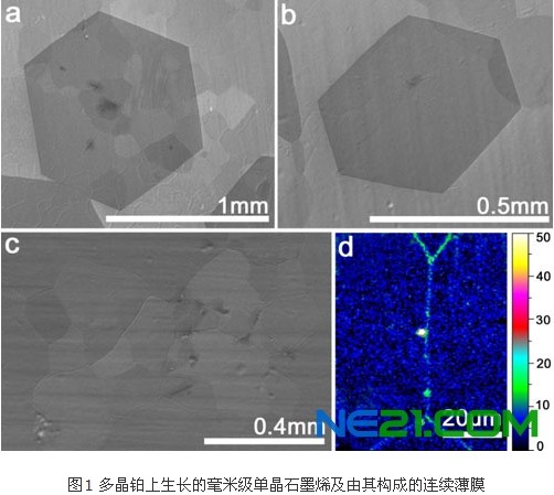 Based on the growth of graphene by the atmospheric pressure CVD method, the researchers of the Institute of Metals proposed the use of noble metal platinum as the growth matrix to realize the preparation of millimeter-sized hexagonal single crystal graphene (Fig. 1), and prepared by the millimeter scale. A graphene film composed of single crystal graphene. It is found that the growth behavior of graphene on polycrystalline platinum and single crystal platinum is similar. The strong catalytic cracking ability of platinum to methane and hydrogen and the use of low concentration methane and high concentration hydrogen in the reaction are to achieve low nucleation density of graphene. The key to the final preparation of large-sized single crystal graphene. Due to the small difference in thermal expansion coefficient between graphene and platinum matrix, the average height of wrinkles on the obtained graphene is only 0.8 nm, which is much smaller than the wrinkles of graphene grown on copper and nickel substrates. They collaborated with the Baoxin and research team of the Dalian Institute of Chemical Physics of the Chinese Academy of Sciences to characterize a single graphene island by low-energy electron diffraction and low-energy electron microscopy. It was found that the graphene islands with regular hexagonal structure are single crystals, and the boundary Graphene islands with concave corners are mostly polycrystalline structures.
 At the same time, they also invented a bubble-free lossless transfer method based on electrochemical gas intercalation to transfer graphene grown on platinum to any substrate (Fig. 2). Unlike the conventional transfer methods based on matrix corrosion, the transfer method has no damage and loss to graphene and platinum matrix, and the platinum matrix can be reused indefinitely. The transferred graphene completely retains its original structure and quality, and no metal impurities remain (Fig. 3). The bubbling transfer method is simple, fast, and non-polluting, and is suitable for transfer of noble metals such as ruthenium and osmium, and graphene grown on common metals such as copper and nickel. The metal matrix can be reused as a low cost. A universal method for rapidly transferring high quality graphene. Raman spectroscopy studies have shown that the single crystal graphene transferred by this method has a high quality (Fig. 4). In turn, they collaborated with the Peng Lianma research team of the Department of Electronics of Peking University to make a single-effect graphene transistor transferred to a Si/SiO2 substrate, and measured the carrier mobility of the single crystal graphene at room temperature. Up to 7100cm2V-1s-1 (Fig. 4), and is expected to be further improved by using a boron nitride matrix. The repeated growth of large-sized single crystal graphene and its thin films on metal substrates is the study of the physical properties of graphene and its material application in the fields of high performance nanoelectronic devices and transparent conductive films. The achievement has been funded by the National Natural Science Foundation of China, the Ministry of Science and Technology, and the Chinese Academy of Sciences. It has applied for 2 Chinese invention patents.
 Based on the growth of graphene by the atmospheric pressure CVD method, the researchers of the Institute of Metals proposed the use of noble metal platinum as the growth matrix to realize the preparation of millimeter-sized hexagonal single crystal graphene (Fig. 1), and prepared by the millimeter scale. A graphene film composed of single crystal graphene. It is found that the growth behavior of graphene on polycrystalline platinum and single crystal platinum is similar. The strong catalytic cracking ability of platinum to methane and hydrogen and the use of low concentration methane and high concentration hydrogen in the reaction are to achieve low nucleation density of graphene. The key to the final preparation of large-sized single crystal graphene. Due to the small difference in thermal expansion coefficient between graphene and platinum matrix, the average height of wrinkles on the obtained graphene is only 0.8 nm, which is much smaller than the wrinkles of graphene grown on copper and nickel substrates. They collaborated with the Baoxin and research team of the Dalian Institute of Chemical Physics of the Chinese Academy of Sciences to characterize a single graphene island by low-energy electron diffraction and low-energy electron microscopy. It was found that the graphene islands with regular hexagonal structure are single crystals, and the boundary Graphene islands with concave corners are mostly polycrystalline structures.

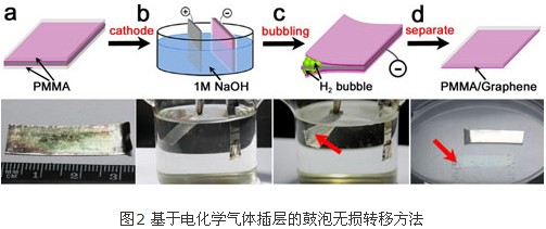
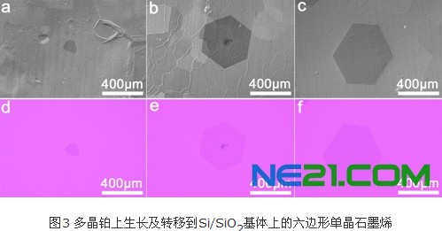
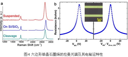
 At the same time, they also invented a bubble-free lossless transfer method based on electrochemical gas intercalation to transfer graphene grown on platinum to any substrate (Fig. 2). Unlike the conventional transfer methods based on matrix corrosion, the transfer method has no damage and loss to graphene and platinum matrix, and the platinum matrix can be reused indefinitely. The transferred graphene completely retains its original structure and quality, and no metal impurities remain (Fig. 3). The bubbling transfer method is simple, fast, and non-polluting, and is suitable for transfer of noble metals such as ruthenium and osmium, and graphene grown on common metals such as copper and nickel. The metal matrix can be reused as a low cost. A universal method for rapidly transferring high quality graphene. Raman spectroscopy studies have shown that the single crystal graphene transferred by this method has a high quality (Fig. 4). In turn, they collaborated with the Peng Lianma research team of the Department of Electronics of Peking University to make a single-effect graphene transistor transferred to a Si/SiO2 substrate, and measured the carrier mobility of the single crystal graphene at room temperature. Up to 7100cm2V-1s-1 (Fig. 4), and is expected to be further improved by using a boron nitride matrix. The repeated growth of large-sized single crystal graphene and its thin films on metal substrates is the study of the physical properties of graphene and its material application in the fields of high performance nanoelectronic devices and transparent conductive films. The achievement has been funded by the National Natural Science Foundation of China, the Ministry of Science and Technology, and the Chinese Academy of Sciences. It has applied for 2 Chinese invention patents.
Bolts And Nuts,Nylock Nut,Eye Bolt,Eye Nut
Taizhou Fengye Metal Products Co., Ltd. , https://www.fyhandware.com