High-power LED packaging mainly involves light, heat, electricity, structure and process, as shown in Figure 1. These factors are mutually independent and affect each other. Among them, the light is the purpose of LED packaging, heat is the key, electricity, structure and technology are the means, and performance is a concrete manifestation of the level of packaging. From the aspect of process compatibility and reducing production costs, the LED package design should be carried out at the same time as the chip design. That is, the chip structure should take into account the package structure and process. Otherwise, after the chip is manufactured, the chip structure may be adjusted due to the needs of the package, thereby prolonging the product development cycle and the process cost, sometimes even impossible.
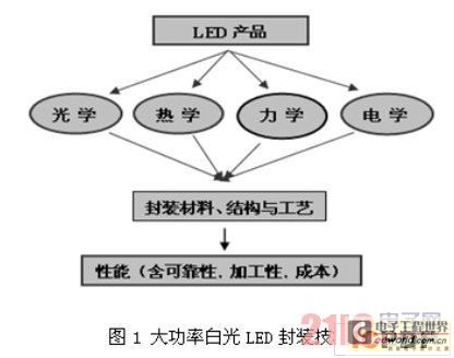
Specifically, the key technologies of high-power LED packaging include: First, the low thermal resistance packaging technology For the existing LED light efficiency level, because about 80% of the input power is converted into heat, and the LED chip area is small, therefore, the chip Heat dissipation is a key issue that LED packaging must address. It mainly includes chip layout, package material selection (substrate material, thermal interface material), process, and heat sink design.
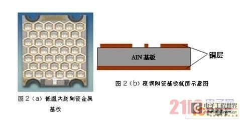
The thermal resistance of the LED package mainly includes the internal thermal resistance and interface thermal resistance of the material (heat-dissipating substrate and heat sink structure). The role of the heat-dissipating substrate is to absorb the heat generated by the chip and conduct it to the heat sink to achieve heat exchange with the outside world. Common heat-dissipating substrate materials include silicon, metals (eg, aluminum, copper), ceramics (eg, AlN, SiC), and composite materials. For example, the third-generation LED of Nichia Corporation adopts CuW as the substrate, flips the 1mm chip on the CuW substrate, reduces the thermal resistance of the package, and improves the luminous power and efficiency; LaminaCeramics Corporation has developed a low-temperature co-fired ceramic metal substrate, As shown in Figure 2(a), the corresponding LED packaging technology has been developed. The technology first prepares a high-power LED chip suitable for eutectic welding and a corresponding ceramic substrate, and then directly solderes the LED chip and the substrate together. Because the eutectic soldering layer, electrostatic protection circuit, drive circuit and control compensation circuit are integrated on the substrate, not only the structure is simple, but also the thermal conductivity is high and the thermal interface is less, which greatly improves the heat dissipation performance and is a high-power LED array package. Presented a solution. The high thermal conductivity copper-clad ceramic board developed by the German company Curmilk is sintered from a ceramic substrate (AlN or) and a conductive layer (Cu) at a high temperature and high pressure. No adhesive is used, so the thermal conductivity is good, the strength is high, and the insulation is strong. , as shown in Figure 2 (b). Aluminum nitride (AlN) has a thermal conductivity of 160 W/mk and a coefficient of thermal expansion (comparable with the thermal expansion coefficient of silicon), which reduces the thermal stress of the package.
Studies have shown that the package interface has a great influence on the thermal resistance. If the interface cannot be handled correctly, it is difficult to obtain a good heat dissipation effect. For example, a well-contacted interface at room temperature may have interfacial gaps at high temperatures, and warping of the substrate may also affect bonding and localized heat dissipation. The key to improving LED packaging is to reduce contact and interface thermal resistance and enhance heat dissipation. Therefore, the choice of thermal interface material (TIM) between the chip and the heat-dissipating substrate is very important. The commonly used TIM of LED package is conductive adhesive and thermal conductive adhesive. Due to low thermal conductivity, it is generally 0, 5-2, 5W/mK, resulting in high thermal resistance of the interface. The use of low-temperature or eutectic solder, solder paste or conductive paste doped with nanoparticles as the thermal interface material can greatly reduce the interface thermal resistance.
Second, the high light rate package structure and process in the use of LED, the radiation generated by the photon generated in the outward emission loss, mainly including three aspects: the chip internal structural defects and the absorption of the material; photon in the exit interface due to refraction The reflection loss due to the rate difference; and the total reflection loss due to the incident angle greater than the total reflection critical angle. Therefore, a lot of light cannot be emitted from the chip to the outside. By coating the surface of the chip with a transparent adhesive layer (encapsulant) with a relatively high refractive index, the adhesive layer is between the chip and the air, thereby effectively reducing the loss of photons at the interface and improving the light extraction efficiency. In addition, the role of potting glue also includes mechanical protection of the chip, stress relief, and as a light guide structure. Therefore, it is required to have high light transmittance, high refractive index, good thermal stability, good fluidity, and easy spraying. In order to improve the reliability of the LED package, it is also required that the potting material has low hygroscopicity, low stress, and aging resistance. Currently used potting compounds include epoxy and silicone. Due to its high light transmittance, high refractive index, good thermal stability, low stress and low hygroscopicity, silica gel is obviously superior to epoxy resin and widely used in high-power LED packaging, but its cost is high. Studies have shown that increasing the refractive index of silica gel can effectively reduce the photon loss caused by the physical barrier of refractive index and improve the external quantum efficiency, but the performance of silica gel is greatly influenced by the ambient temperature. As the temperature rises, the thermal stress inside the silica gel increases, causing the refractive index of the silica gel to decrease, thereby affecting the light efficiency and light intensity distribution of the LED.
Phosphor's function is to combine light and color to form white light. Its characteristics mainly include particle size, shape, luminous efficiency, conversion efficiency, stability (heat and chemical), etc. Among them, luminous efficiency and conversion efficiency are the key. Studies have shown that as the temperature rises, the quantum efficiency of the phosphor decreases, the amount of emitted light decreases, and the wavelength of radiation also changes, resulting in changes in the color temperature and chromaticity of the white LED. Higher temperatures also accelerate the aging of the phosphor. The reason is that the phosphor coating layer is made of epoxy or silica gel and phosphor powder, and the heat dissipation performance is poor. When it is irradiated by violet light or ultraviolet light, it is prone to temperature quenching and aging, which reduces the luminous efficiency. In addition, the thermal stability of encapsulants and phosphors at high temperatures is also problematic. Because the commonly used phosphor size is above 1um, the refractive index is greater than or equal to 1, 85, and the refractive index of silica gel is generally around 1,5. Due to the mismatch of the refractive index between the two, and the size of the phosphor particles is much larger than the light scattering limit (30 nm), there is light scattering on the surface of the phosphor particles, which reduces the light extraction efficiency. By incorporating nano-phosphor powder in silica gel, the refractive index can be increased to 1,8 or more, light scattering can be reduced, the LED light-emitting efficiency (10%-20%) can be improved, and light-color quality can be effectively improved.
The traditional phosphor coating method is to mix the phosphor with the potting glue and then apply it on the chip. Due to the inability to precisely control the thickness and shape of the phosphor coating, the color of the emitted light is inconsistent and blue or yellowish light appears. The Conformalcoating technology developed by Lumileds Co., Ltd. can achieve even coating of phosphors and ensure the uniformity of light color, as shown in Figure 3(b). However, studies have shown that when the phosphor is directly coated on the surface of the chip, light emission efficiency is low due to the presence of light scattering. In view of this, the Rensselaer Institute of the United States has proposed a Scattered Photon Extraction Method (SPE) to improve the device by arranging a focusing lens on the surface of the chip and placing the glass sheet containing the phosphor at a certain distance from the chip. Reliability, but also greatly improved light efficiency (60%), as shown in Figure 3 (c).
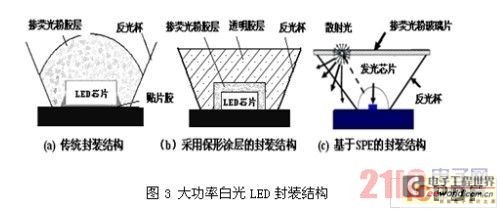
In general, in order to improve the light emitting efficiency and reliability of the LED, the encapsulating layer is gradually replaced by a high-refractive transparent glass or glass-ceramics, and is not only improved by doping or coating the phosphor on the surface of the glass. Phosphor uniformity, but also improve the packaging efficiency. In addition, reducing the number of optical interfaces of the LED's light output direction is also an effective measure to increase the light output efficiency. Third, array packaging and system integration technology After 40 years of development, LED packaging technology and structure has gone through four stages, as shown in Figure 4.
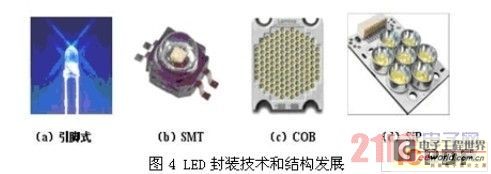
1ã€Lamp LED package is a commonly used 3-5mm package structure. It is generally used for LED package with small current (20-30mA) and low power (less than 0, 1W). It is mainly used for meter display or indication, and can also be used as a display screen when integrated in large scale. The disadvantage is that the package has a large thermal resistance (usually higher than 100K/W) and a shorter lifetime. 2. Surface Mount (SMT-LED) Package Surface Mount Technology (SMT) is a packaging technology that can directly attach a packaged device to a specified location on the surface of the PCB. Specifically, a specific tool or device is used to align the pins of the chip with pad patterns that are pre-coated with adhesive and solder paste, and then directly mounted on the surface of the PCB that has not been drilled with the mounting hole and then subjected to wave soldering. Or after reflow, establish a reliable mechanical and electrical connection between the device and the circuit. SMT technology has the advantages of high reliability, high frequency characteristics, and easy automation. It is the most popular packaging technology and process in the electronics industry. 3. On-chip COB LED package COB is the English abbreviation of ChipOnBoard. It is an LED chip directly pasted on a PCB board through an adhesive or solder, and then passed through the wire bond. The packaging technology that realizes the electrical interconnection between the chip and the PCB. The PCB board can be a low-cost FR-4 material (glass fiber-reinforced epoxy resin), or it can be a highly thermally conductive metal-based or ceramic-based composite material (such as an aluminum substrate or a copper-clad ceramic substrate, etc.). The wire bonding may use thermosonic bonding at high temperature (gold ball bonding) and ultrasonic bonding at normal temperature (aluminum file welding). COB technology is mainly used for high-power multi-chip array LED packages. Compared with SMT, it not only greatly increases the package power density, but also reduces the package thermal resistance (generally 6-12 W/m, K). 4. System-package (SiP) LED package SiP (System in Package) is a requirement for the portable development and system miniaturization of the complete machine in recent years. The system chip power supply, control circuit, optical microstructure, and sensors are integrated in the system chip. Together, build a more complex and complete system. Compared with other package structures, SiP has good process compatibility (which can use existing electronic packaging materials and processes), high integration, low cost, can provide more new features, easy block testing, short development cycle, etc. . According to different types of technology, SiP can be divided into four types: chip-stacked, module-based, MCM-type and three-dimensional (3D) packaged.
Currently, high-brightness LED devices have to replace incandescent lamps and high-pressure mercury lamps, and must increase the total luminous flux, or the luminous flux that can be utilized. The increase in luminous flux can be achieved by increasing integration, increasing current density, and using large-size chips. These will increase the power density of the LED, such as poor heat dissipation, which will cause the junction temperature of the LED chip to rise, which will directly affect the performance of the LED device (such as reduced luminous efficiency, red-shifted emission light, and reduced lifetime). Multi-chip array packaging is currently one of the most feasible solutions for achieving high luminous flux, but the density of LED array packages is limited by the price, available space, electrical connections, and especially heat dissipation. Due to the high-density integration of the light emitting chip, the temperature on the heat-dissipating substrate is high, and an effective heat sink structure and a suitable packaging process must be adopted. Commonly used heat sink structures are divided into passive and active heat dissipation. Passive heat dissipation generally uses fins with a high riblination coefficient to dissipate heat to the environment through natural convection between the fins and the air. The scheme is simple in structure and high in reliability, but due to the low natural natural convection heat transfer coefficient, it is only suitable for low power density and low integration. For high-power LED packages, active heat dissipation must be used, such as fin + fan, heat pipe, liquid forced convection, micro-channel cooling, phase change cooling, and so on.
In terms of system integration, Taiwan's Xinqiang Optoelectronics adopted system packaging technology (SiP) and used fins and heat pipes in conjunction with high-efficiency heat-dissipating modules to create 72W and 80W high-brightness white LED light sources, as shown in Figure 5(a). ). Due to the lower package thermal resistance (4,38°C/W), when the ambient temperature is 25°C, the LED junction temperature is controlled below 60°C, thus ensuring the service life of the LED and good light emitting performance. Huazhong University of Science and Technology uses the COB package and micro-spray active cooling technology to encapsulate 220W and 1500W ultra-high power LED white light sources, as shown in Figure 5(b).
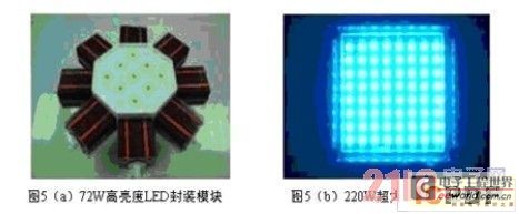
Fig. 5 IV. Packaging Large Production Technology Wafer bonding technology means that the fabrication and packaging of the chip structure and the circuit are all performed on a Wafer. After the package is completed, the wafer is cut to form a single chip. The corresponding die bonding means that after the chip structure and circuit are completed on the wafer, the die is cut to form a die, and then the individual chips are packaged (similar to the current LED packaging process), as shown in FIG. Show. Obviously, wafer bonding packages are more efficient and of higher quality. Since the packaging cost accounts for a large proportion of the LED device manufacturing cost, changing the existing LED package form (from chip bonding to wafer bonding) will greatly reduce the package manufacturing cost. In addition, the wafer bonding package can also improve the cleanliness of LED device production, prevent the dicing and singulation processes before the bonding, and damage the device structure, and improve the package yield and reliability. Therefore, it is an effective way to reduce the packaging cost. means.
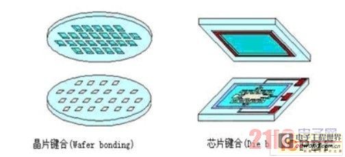
Figure 6 In addition, for high-power LED packages, package-less packaging must be used as much as possible during chip design and package design, while simplifying package structure and minimizing thermal and optical interface counts. Reduce the thermal resistance of the package and improve the light output efficiency.
V. Package Reliability Testing and Evaluation Failure modes of LED devices mainly include electrical failure (such as short circuit or open circuit), light failure (such as high temperature caused by potting yellowing, optical performance degradation, etc.) and mechanical failure (such as lead fracture, Solder removal, etc., and these factors are all related to the package structure and process. The service life of an LED is defined by the mean time to failure (MTTF). For lighting applications, the output light flux of an LED is generally reduced to the initial 70% (usually defined as 50% of the initial value for display use). Due to the long life of the LED, the method of accelerating the environmental test is usually used for reliability testing and evaluation. The test contents mainly include high temperature storage (100°C, 1000h), low temperature storage (-55°C, 1000h), high temperature and high humidity (85°C/85%, 1000h), high and low temperature cycles (85°C to -55°C), thermal shock , corrosion resistance, solvent resistance, mechanical impact and so on. However, accelerating the environmental test is only one aspect of the problem. Research on the prediction mechanism and method of the LED lifetime is still a problem to be studied.
The made-in-China F Series mud pumps can meet the requirements of the same manufacturing technique and quality level as those of F series mud pumps of LTV Co. They feature advanced structural design, reliable use, easy maintenance and compact occupied area. Now, F series mud pumps (from F-500 to F-1600) have been produced in batches and sold to many abroad oilfields. Your order for F series mud pumps is cordially welcome.
The company provides various centrifugal pumps, chemical pumps, screw pumps, booster pumps, variable frequency constant pressure pumps, hydrochloric acid pumps, testing pumps, etc.
Mud Pump,Water Pumps,Booster Pumps,Solar Booster Pump
Rugao Yaou Import & Export Trade Co., Ltd , https://www.ntyaous.com